


SmartSens Showcases Innovative Solutions Across Sensing, Interconnection, and Computing at Electronica Shanghai 2026
2026-7-1
At Electronica Shanghai 2026, held July 1-3 at the Shanghai New International Expo Centre, under the theme of “Sensing · Interconnection · Computing”, SmartSens Technology (Shanghai) Co., Ltd. (SSE STAR MARKET: 688213), a technologically advanced CMOS image sensor supplier, showcased a comprehensive portfolio of new products and solutions spanning industrial machine vision image sensors, high-performance AI vision processing SoCs, and next-generation high-speed optical interconnects solutions.
The showcase marked a major milestone in SmartSens’ innovation journey following the launch of its “3+AI” strategy, highlighting the company’s continued expansion of its technology capabilities and application portfolio.

High-Precision Sensing for Industrial AI Inspection
For intelligent transportation applications, SmartSens showcased the SC1435HGS, a 14MP high-performance global shutter CMOS image sensor, built on SmartSens’ SmartGS™-2 Plus platform and equipped with Lightbox IR® NIR enhancement technology. SC1435HGS combines high sensitivity, high dynamic range, high frame rates, and low noise. With an optimized resolution of 4480H × 3072V, the expanded horizontal coverage enables a single camera to reliably monitor five-lane urban roads, significantly eliminating blind spots and providing intelligent transportation system (ITS) with clear and comprehensive image data for reliable visual perception.

High-Performance Intelligent Transportation Application Demonstration
As industries including printing, textiles, and metal processing continue to accelerate their intelligent transformation, production lines are placing increasingly stringent demands on inspection accuracy, throughput, and reliability. Line-scan CMOS image sensors have become a critical imaging component for high-speed and high-precision inspection of continuous materials. At Electronica Shanghai 2026, SmartSens demonstrated the SC835LA, an 8K ultra-high-resolution, high-speed linear CMOS image sensor, through a patterned fabric roller application. Built on the SmartClarity®-3 technology, SC835LA incorporates an upgraded BSI technology and mask stitching process, delivering high line rates, high sensitivity, low power consumption, and low noise. Available in both monochrome and color versions, SC835LA combines excellent image quality with high-speed data transmission, making it well-suited for high-speed inspection of long, continuous materials in intelligent industrial production lines and other demanding machine vision applications.

High-End Industrial Line-Scan Camera Application Demonstration
SmartSens also showcased a range of advanced products and application solutions, including the SC4880RS CIS for industrial cameras, which features an ultra-large optical format and ultra-high resolution, the 12MP SC1220IOT CIS for AI glasses, and the 2MP SC1400ME CIS for ultra-compact medical applications. Together, these products demonstrate SmartSens’ deep technology expertise and expanding product portfolio in industrial machine vision and other emerging applications.
High-Speed Optical Interconnects for High-Bandwidth Data Transmission
The next-generation high-speed optical interconnects solution from SmartSens is unveiled for the first time, marking the second key segment of this exhibition. The solution uses MicroLED as the light source in place of lasers. Leveraging the non-laser spontaneous emission characteristics of MicroLED, the solution can increase optoelectronic conversion efficiency by 30%, improving overall system power efficiency and helping address the power consumption challenges of high-performance computing systems operating continuously at scale. Designed for short-reach communication of up to 50 meters, the solution targets chip-to-chip and board-to-board interconnect applications. It natively supports fully parallel GPU/HBM interconnect protocols and adopts an architecture integrating the light source, direct modulation, and direct signal connection to enable precise physical-layer interface matching. The solution is designed to support high-throughput data transmission within computing clusters, enabling to address band applications in AI data centers, ADAS, and advanced industrial vision.
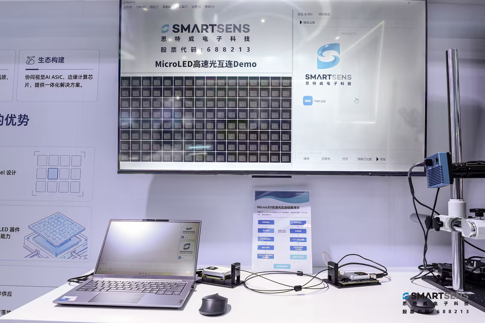
High-Speed Optical Interconnects Prototype Demonstration
To address transmission performance bottlenecks in conventional electrical interconnect architectures, the solution adopts a parallel MicroLED optical transmission architecture capable of supporting an aggregate parallel bandwidth of more than 1 Tbps. By replacing a limited number of high-speed electrical channels with hundreds of parallel low-speed optical channels, the architecture is designed to address key challenges of electrical interconnects, including bandwidth limitations, high power consumption, signal crosstalk, and restricted transmission distance. On-site demonstrations showed that the transmission rate of a single MicroLED channel has exceeded 3 Gbps, while typical power consumption can be as low as 0.8 pJ/bit, combining high-speed transmission with low power consumption.
“Optical interconnection is an important foundation for the continued development of the computing industry, and the localization of core optical interconnection technologies is an inevitable trend,” said Vincent Wang, Co-General Manager of SmartSens’ HOC Business Group. “Since the beginning of its strategic layout, SmartSens has been committed to an open and collaborative approach, working closely with partners across the industry chain to advance the development of short-reach optical interconnection technologies in China. We aim to help strengthen the domestic technology ecosystem and support the high-quality, self-reliant development of China’s semiconductor and computing industries.” Vincent Wang also mentioned that SmartSens’ MicroLED-based high-speed optical interconnects solution is expected to reach commercial deployment in 2027.

MicroLED Real-Time Eye Diagram at 3Gbps Single-Channel Transmission Rate
Intelligent Computing for Edge AI Vision
Focusing on lightweight AI edge computing, SmartSens’ sub-brand Flyingchip showcased M2, the next-generation automotive vision processing SoC. M2 features a dual-domain architecture integrating a quad-core ARM® Cortex®-A53 CPU with a dual-core ARM® Cortex®-R52+ MCU, augmented with a proprietary FlyingMatrix™ NPU delivering up to 10 TOPS of AI computing performance. Its powerful multi-model parallel inference capabilities enable simultaneous processing of multiple camera inputs. Built on a dense computing architecture, M2 supports end-to-end processing of high-definition automotive vision data. It performs computation across multiple high-definition image streams for applications including surround view, front view, and in-cabin monitoring, preserving image details and supporting reliable visual perception for smart driving. M2 also features proprietary FlyingSight™ AI-ISP, which reduces repeated memory read/write operations during image processing, thereby lowering processing latency and overall system power consumption. It also better supports advanced imaging functions such as HDR synthesis and 2D/3D noise reduction, further enhancing image quality. M2 complies with the AEC-Q100 Grade 2 automotive standard and ISO 26262 ASIL-B functional safety level. It is designed for a broad range of automotive vision applications, including L2 front-view all-in-one camera, CMS & E-mirror, DMS & OMS, and HD surround-view systems.
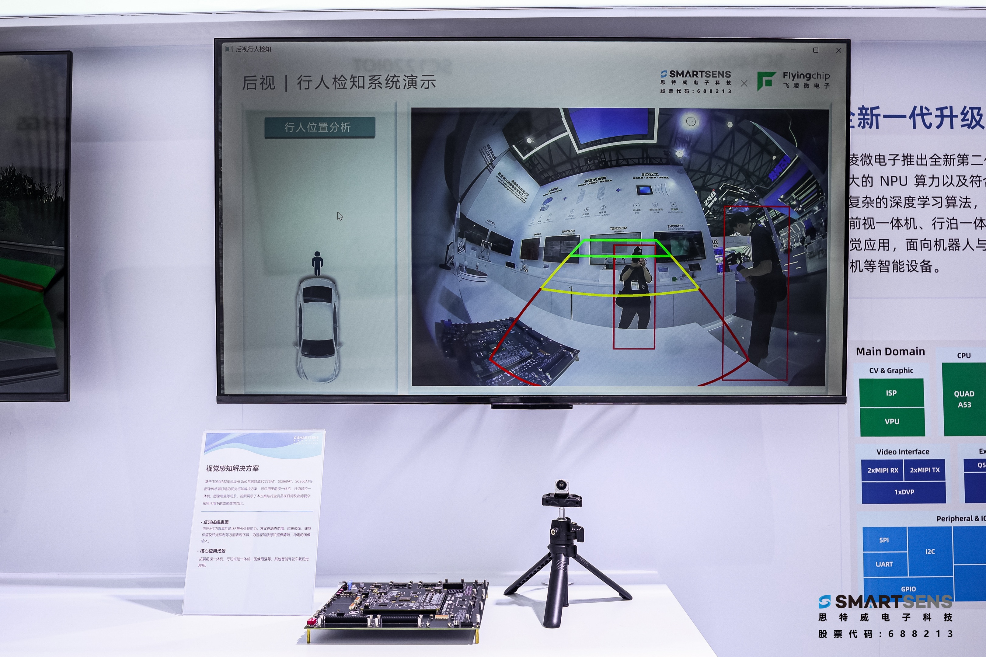
Flyingchip Rear-View Detection Live Demonstration
Flyingchip also unveils A2, an AI vision processing SoC designed for robotics and industrial vision applications. A2 supports simultaneous input from four cameras and integrates a hardware DPU for binocular depth computation. Equipped with the proprietary FlyingMatix™ NPU, it is capable of processing multiple AI algorithms in parallel, including image segmentation, obstacle avoidance, and VSLAM localization. By integrating visual perception and AI processing capabilities into a single platform, A2 is designed to enable high-precision visual perception and reliable, real-time, and safe control for intelligent machines.

Flyingchip A2 SoC Binocular Real-Time Depth Map Demonstration
SmartSens has remained committed to advancing high-end imaging technologies through continuous R&D and innovation since its establishment. Guided by its “3+AI” strategy, SmartSens is building an closed-loop technology framework spanning high-precision sensing, high-speed interconnection, and intelligent computing, while accelerating the convergence of these three core technology domains with AI. While consolidating its flagship CIS businesses in automotive, security, and consumer electronics, SmartSens is also expanding into emerging markets including industrial vision, optical interconnection, and edge AI SoCs. Through these efforts, the company is continuously enhancing its full-stack technology capabilities and expanding its diversified product ecosystem.
Leveraging proprietary technologies and innovation, SmartSens is committed to advancing imaging and semiconductor technologies and providing the “core” capabilities for the intelligent and digital transformation of industries. Spanning diverse sectors, SmartSens aims to empower the high-quality development of intelligent manufacturing and drive the growth of the digital economy.
Related News
SmartSens Showcases Innovative Solutions Across Sensing, Interconnection, and Computing at Electronica Shanghai 2026
Learn More >
SmartSens Technology Brings New Innovation, New World and New Future to CPSE 2019
Learn More >
Chips Change Machine Vision World - SmartSens Stands Shining in ITE 2018
Learn More >
The Era of Smart Chip - 2018 Security China
Learn More >